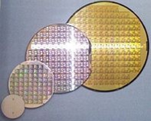
▌GaN EPI Wafer Features
GaN EPI Wafer is a new type of semiconductor material that is widely used in applications such as high power, high frequency, and high temperature due to its unique physical properties. Compared to traditional semiconductor materials, GaN EPI Wafer has higher electron mobility, smaller resistance, and higher thermal stability, which enables more efficient energy conversion and more reliable performance.
As a company dedicated to semiconductor technology innovation, we have been paying attention to the development and application of new technologies and investing resources in research and innovation. Our GaN EPI Wafer products have been successfully applied in multiple high-end fields such as lidar, 5G base stations, and high-power supplies.
In summary, our GaN EPI Wafer products have been widely used and recognized in the semiconductor technology field. We will continue to optimize and improve our products and solutions to meet the needs and expectations of our customers and provide them with better products and services.
As a supplier of GaN EPI Wafer products, we not only provide high-quality products but also offer complete solutions to meet the needs and expectations of our customers. We have a professional technical team and modern production equipment that can provide a full range of solutions from research, design, production, to after-sales service, thereby ensuring the success of our customers and the quality of our products.
| 圖片 | P/N | Size | Barrier Layer AL Composition | FWHM (0002) Arcsec | Total EPI Thickness (nm) | Wafer Bowing (um) | Particle Count (ea) | |
|---|---|---|---|---|---|---|---|---|
 | 000S06EP01 | 6" EPI | ~750 | 4200 ±10% | +/-50um | ~500 | ||
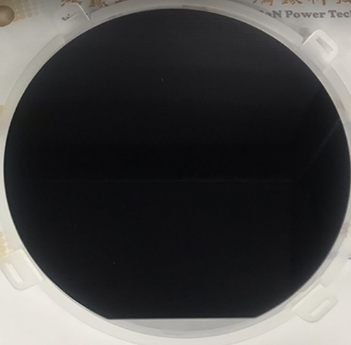 | 000S08EP01 | 8" EPI | ~750 | 4200 ±10% | +/-80um | ~500 |